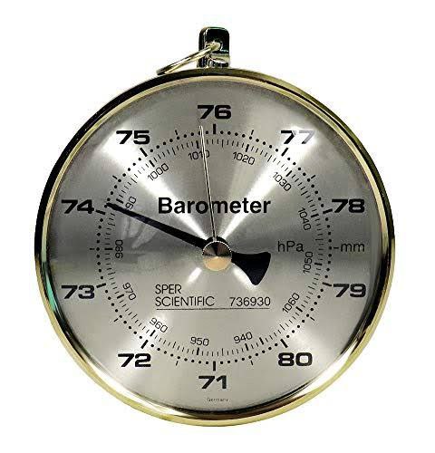
A barometer is a scientific instrument that is used to measure air pressure in a certain environment. Pressure tendency can forecast short term changes in the weather. Many measurements of air pressure are used within surface weather analysis to help find surface troughs, pressure systems and frontal boundaries.
━━━━━━━━━━━━
☢ @Physics ⚡| @Education 📖
━━━━━━━━━━━━
☢ @Physics ⚡| @Education 📖
👍40❤11🔥11🤩4
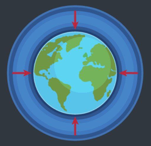
Atmospheric pressure, also known as barometric pressure (after the barometer), is the pressure within the atmosphere of Earth. The standard atmosphere (symbol: atm) is a unit of pressure defined as 101,325 Pa (1,013.25 hPa), which is equivalent to 1013.25 millibars, 760 mm Hg, 29.9212 inches Hg, or 14.696 psi. The atm unit is roughly equivalent to the mean sea-level atmospheric pressure on Earth; that is, the Earth's atmospheric pressure at sea level is approximately 1 atm.
In most circumstances, atmospheric pressure is closely approximated by the hydrostatic pressure caused by the weight of air above the measurement point. As elevation increases, there is less overlying atmospheric mass, so that atmospheric pressure decreases with increasing elevation. Because the atmosphere is thin relative to the Earth's radius—especially the dense atmospheric layer at low altitudes—the Earth's gravitational acceleration as a function of altitude can be approximated as constant and contributes little to this fall off. Pressure measures force per unit area, with SI units of pascals (1 pascal = 1 newton per square metre, 1 N/m²). On average, a column of air with a cross-sectional area of 1 square centimetre (cm²), measured from mean (average) sea level to the top of Earth's atmosphere, has a mass of about 1.03 kilogram and exerts a force or "weight" of about 10.1 newtons, resulting in a pressure of 10.1 N/cm² or 101 kN/m² (101 kilopascals, kPa). A column of air with a cross-sectional area of 1 in² would have a weight of about 14.7 lbf, resulting in a pressure of 14.7 lbf/in².
━━━━━━━━━━━━
☢ @Physics ⚡| @Education 📖
In most circumstances, atmospheric pressure is closely approximated by the hydrostatic pressure caused by the weight of air above the measurement point. As elevation increases, there is less overlying atmospheric mass, so that atmospheric pressure decreases with increasing elevation. Because the atmosphere is thin relative to the Earth's radius—especially the dense atmospheric layer at low altitudes—the Earth's gravitational acceleration as a function of altitude can be approximated as constant and contributes little to this fall off. Pressure measures force per unit area, with SI units of pascals (1 pascal = 1 newton per square metre, 1 N/m²). On average, a column of air with a cross-sectional area of 1 square centimetre (cm²), measured from mean (average) sea level to the top of Earth's atmosphere, has a mass of about 1.03 kilogram and exerts a force or "weight" of about 10.1 newtons, resulting in a pressure of 10.1 N/cm² or 101 kN/m² (101 kilopascals, kPa). A column of air with a cross-sectional area of 1 in² would have a weight of about 14.7 lbf, resulting in a pressure of 14.7 lbf/in².
━━━━━━━━━━━━
☢ @Physics ⚡| @Education 📖
🔥24👍16❤9🤩6
Quantum superposition is a fundamental principle of quantum mechanics. It states that, much like waves in classical physics, any two (or more) quantum states can be added together ("superposed") and the result will be another valid quantum state; and conversely, that every quantum state can be represented as a sum of two or more other distinct states. Mathematically, it refers to a property of solutions to the Schrödinger equation; since the Schrödinger equation is linear, any linear combination of solutions will also be a solution(s). An example of a physically observable manifestation of the wave nature of quantum systems is the interference peaks from an electron beam in a double-slit experiment. The pattern is very similar to the one obtained by diffraction of classical waves.
━━━━━━━━━━━━
☢ @Physics ⚡| @Education 📖
━━━━━━━━━━━━
☢ @Physics ⚡| @Education 📖
👍33🔥18❤7😱5🤩5
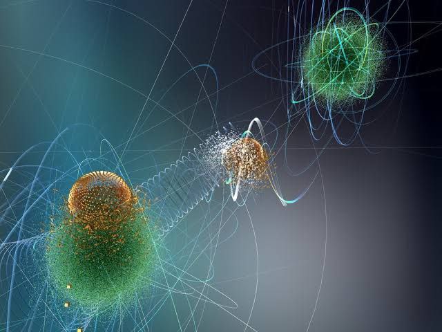
▶️ Quantum teleportation is a technique for transferring quantum information from a sender at one location to a receiver some distance away. While teleportation is commonly portrayed in science fiction as a means to transfer physical objects from one location to the next, quantum teleportation only transfers quantum information. The sender does not have to know the particular quantum state being transferred. Moreover, the location of the recipient can be unknown, but to complete the quantum teleportation, classical information needs to be sent from sender to receiver. Because classical information needs to be sent, quantum teleportation cannot occur faster than the speed of light.
▶️ One of the first scientific articles to investigate quantum teleportation is "Teleporting an Unknown Quantum State via Dual Classical and Einstein-Podolsky-Rosen Channels" published by C. H. Bennett, G. Brassard, C. Crépeau, R. Jozsa, A. Peres, and W. K. Wootters in 1993, in which they used dual communication methods to send/receive quantum information. It was experimentally realized in 1997 by two research groups, led by Sandu Popescu and Anton Zeilinger, respectively.
▶️ Experimental determinations of quantum teleportation have been made in information content - including photons, atoms, electrons, and superconducting circuits - as well as distance with 1,400 km (870 mi) being the longest distance of successful teleportation by the group of Jian-Wei Pan using the Micius satellite for space-based quantum teleportation.
━━━━━━━━━━━━
☢ @Physics ⚡| @Education 📖
▶️ One of the first scientific articles to investigate quantum teleportation is "Teleporting an Unknown Quantum State via Dual Classical and Einstein-Podolsky-Rosen Channels" published by C. H. Bennett, G. Brassard, C. Crépeau, R. Jozsa, A. Peres, and W. K. Wootters in 1993, in which they used dual communication methods to send/receive quantum information. It was experimentally realized in 1997 by two research groups, led by Sandu Popescu and Anton Zeilinger, respectively.
▶️ Experimental determinations of quantum teleportation have been made in information content - including photons, atoms, electrons, and superconducting circuits - as well as distance with 1,400 km (870 mi) being the longest distance of successful teleportation by the group of Jian-Wei Pan using the Micius satellite for space-based quantum teleportation.
━━━━━━━━━━━━
☢ @Physics ⚡| @Education 📖
🔥35👍17❤4🤩3😱1
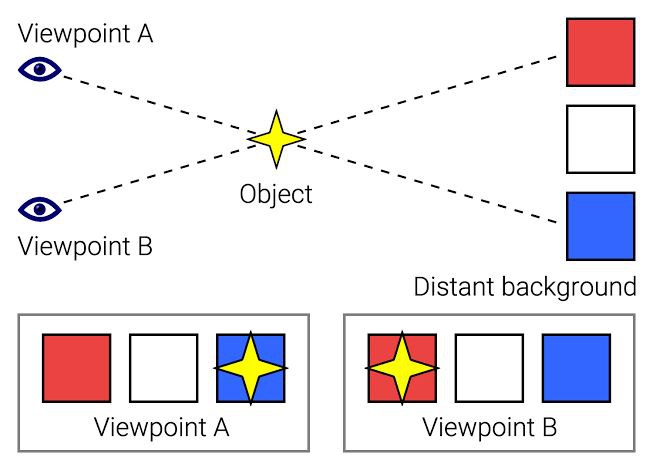
▶️ Parallax is a displacement or difference in the apparent position of an object viewed along two different lines of sight, and is measured by the angle or semi-angle of inclination between those two lines. Due to foreshortening, nearby objects show a larger parallax than farther objects when observed from different positions, so parallax can be used to determine distances.
▶️ To measure large distances, such as the distance of a planet or a star from Earth, astronomers use the principle of parallax. Here, the term parallax is the semi-angle of inclination between two sight-lines to the star, as observed when Earth is on opposite sides of the Sun in its orbit. These distances form the lowest rung of what is called "the cosmic distance ladder", the first in a succession of methods by which astronomers determine the distances to celestial objects, serving as a basis for other distance measurements in astronomy forming the higher rungs of the ladder.
▶️ Parallax also affects optical instruments such as rifle scopes, binoculars, microscopes, and twin-lens reflex cameras that view objects from slightly different angles. Many animals, along with humans, have two eyes with overlapping visual fields that use parallax to gain depth perception; this process is known as stereopsis. In computer vision the effect is used for computer stereo vision, and there is a device called a parallax rangefinder that uses it to find range, and in some variations also altitude to a target.
━━━━━━━━━━━━
☢ @Physics ⚡| @Education 📖
▶️ To measure large distances, such as the distance of a planet or a star from Earth, astronomers use the principle of parallax. Here, the term parallax is the semi-angle of inclination between two sight-lines to the star, as observed when Earth is on opposite sides of the Sun in its orbit. These distances form the lowest rung of what is called "the cosmic distance ladder", the first in a succession of methods by which astronomers determine the distances to celestial objects, serving as a basis for other distance measurements in astronomy forming the higher rungs of the ladder.
▶️ Parallax also affects optical instruments such as rifle scopes, binoculars, microscopes, and twin-lens reflex cameras that view objects from slightly different angles. Many animals, along with humans, have two eyes with overlapping visual fields that use parallax to gain depth perception; this process is known as stereopsis. In computer vision the effect is used for computer stereo vision, and there is a device called a parallax rangefinder that uses it to find range, and in some variations also altitude to a target.
━━━━━━━━━━━━
☢ @Physics ⚡| @Education 📖
🔥31👍24❤3🎉2😁1😱1
A Wheatstone bridge is an electrical circuit used to measure an unknown electrical resistance by balancing two legs of a bridge circuit, one leg of which includes the unknown component. The primary benefit of the circuit is its ability to provide extremely accurate measurements (in contrast with something like a simple voltage divider). Its operation is similar to the original potentiometer. The Wheatstone bridge was invented by Samuel Hunter Christie (sometimes spelled "Christy") in 1833 and improved and popularized by Sir Charles Wheatstone in 1843. One of the Wheatstone bridge's initial uses was for soil analysis and comparison.
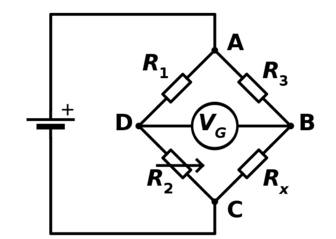
Below is the wheatstone bridge circuit diagram. The unknown resistance Rₓ is to be measured; resistances R₁, R₂ and R₃ are known, where R₂ is adjustable. When the measured voltage Vg is 0, both legs have equal voltage ratios: R₂/R₁ = Rₓ/R₃ and Rₓ = R₃R₂/R₁.
━━━━━━━━━━━━
☢ @Physics ⚡| @Education 📖
Below is the wheatstone bridge circuit diagram. The unknown resistance Rₓ is to be measured; resistances R₁, R₂ and R₃ are known, where R₂ is adjustable. When the measured voltage Vg is 0, both legs have equal voltage ratios: R₂/R₁ = Rₓ/R₃ and Rₓ = R₃R₂/R₁.
━━━━━━━━━━━━
☢ @Physics ⚡| @Education 📖
👍40❤10🔥8🤩1
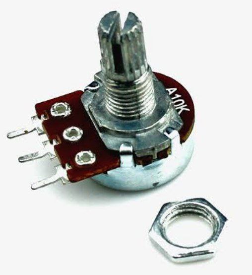
▶️ A potentiometer is an instrument for measuring voltage or 'potential difference' by comparison of an unknown voltage with a known reference voltage. If a sensitive indicating instrument is used, very little current is drawn from the source of the unknown voltage. Since the reference voltage can be produced from an accurately calibrated voltage divider, a potentiometer can provide high precision in measurement. The method was described by Johann Christian Poggendorff around 1841 and became a standard laboratory measuring technique.
▶️ In this arrangement, a fraction of a known voltage from a resistive slide wire is compared with an unknown voltage by means of a galvanometer. The sliding contact or wiper of the potentiometer is adjusted and the galvanometer briefly connected between the sliding contact and the unknown voltage. The deflection of the galvanometer is observed and the sliding tap adjusted until the galvanometer no longer deflects from zero. At that point the galvanometer draws no current from the unknown source, and the magnitude of voltage can be calculated from the position of the sliding contact.
▶️ This null balance measuring method is still important in electrical metrology and standards work and is also used in other areas of electronics.
━━━━━━━━━━━━
☢ @Physics ⚡| @Education 📖
▶️ In this arrangement, a fraction of a known voltage from a resistive slide wire is compared with an unknown voltage by means of a galvanometer. The sliding contact or wiper of the potentiometer is adjusted and the galvanometer briefly connected between the sliding contact and the unknown voltage. The deflection of the galvanometer is observed and the sliding tap adjusted until the galvanometer no longer deflects from zero. At that point the galvanometer draws no current from the unknown source, and the magnitude of voltage can be calculated from the position of the sliding contact.
▶️ This null balance measuring method is still important in electrical metrology and standards work and is also used in other areas of electronics.
━━━━━━━━━━━━
☢ @Physics ⚡| @Education 📖
👍37🔥9❤6😱1
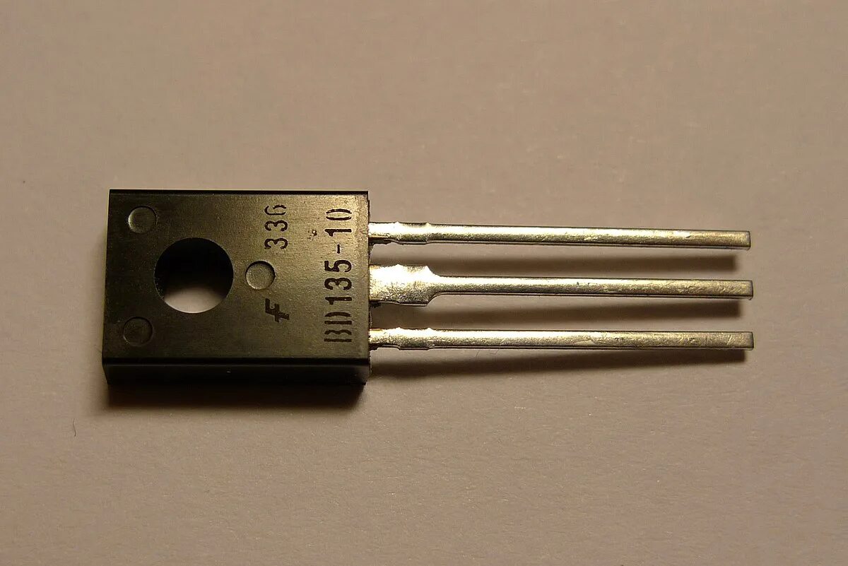
▶️ A transistor is a semiconductor device used to amplify or switch electrical signals and power. The transistor is one of the basic building blocks of modern electronics. It is composed of semiconductor material, usually with at least three terminals for connection to an electronic circuit. A voltage or current applied to one pair of the transistor's terminals controls the current through another pair of terminals. Because the controlled (output) power can be higher than the controlling (input) power, a transistor can amplify a signal. Some transistors are packaged individually, but many more are found embedded in integrated circuits.
▶️ Austro-Hungarian physicist Julius Edgar Lilienfeld proposed the concept of a field-effect transistor in 1926, but it was not possible to actually construct a working device at that time. The first working device to be built was a point-contact transistor invented in 1947 by American physicists John Bardeen and Walter Brattain while working under William Shockley at Bell Labs. The three shared the 1956 Nobel Prize in Physics for their achievement. The most widely used type of transistor is the metal–oxide–semiconductor field-effect transistor (MOSFET), which was invented by Mohamed Atalla and Dawon Kahng at Bell Labs in 1959. Transistors revolutionized the field of electronics, and paved the way for smaller and cheaper radios, calculators, and computers, among other things.
▶️ Most transistors are made from very pure silicon, and some from germanium, but certain other semiconductor materials are sometimes used. A transistor may have only one kind of charge carrier, in a field-effect transistor, or may have two kinds of charge carriers in bipolar junction transistor devices. Compared with the vacuum tube, transistors are generally smaller and require less power to operate. Certain vacuum tubes have advantages over transistors at very high operating frequencies or high operating voltages. Many types of transistors are made to standardized specifications by multiple manufacturers.
━━━━━━━━━━━━
☢ @Physics ⚡| @Education 📖
▶️ Austro-Hungarian physicist Julius Edgar Lilienfeld proposed the concept of a field-effect transistor in 1926, but it was not possible to actually construct a working device at that time. The first working device to be built was a point-contact transistor invented in 1947 by American physicists John Bardeen and Walter Brattain while working under William Shockley at Bell Labs. The three shared the 1956 Nobel Prize in Physics for their achievement. The most widely used type of transistor is the metal–oxide–semiconductor field-effect transistor (MOSFET), which was invented by Mohamed Atalla and Dawon Kahng at Bell Labs in 1959. Transistors revolutionized the field of electronics, and paved the way for smaller and cheaper radios, calculators, and computers, among other things.
▶️ Most transistors are made from very pure silicon, and some from germanium, but certain other semiconductor materials are sometimes used. A transistor may have only one kind of charge carrier, in a field-effect transistor, or may have two kinds of charge carriers in bipolar junction transistor devices. Compared with the vacuum tube, transistors are generally smaller and require less power to operate. Certain vacuum tubes have advantages over transistors at very high operating frequencies or high operating voltages. Many types of transistors are made to standardized specifications by multiple manufacturers.
━━━━━━━━━━━━
☢ @Physics ⚡| @Education 📖
👍37❤12🔥4🎉3
A semiconductor material has an electrical conductivity value falling between that of a conductor, such as metallic copper, and an insulator, such as glass. Its resistivity falls as its temperature rises; metals behave in the opposite way. Its conducting properties may be altered in useful ways by introducing impurities ("doping") into the crystal structure. When two differently doped regions exist in the same crystal, a semiconductor junction is created. The behavior of charge carriers, which include electrons, ions, and electron holes, at these junctions is the basis of diodes, transistors, and most modern electronics. Some examples of semiconductors are silicon, germanium, gallium arsenide, and elements near the so-called "metalloid staircase" on the periodic table. After silicon, gallium arsenide is the second-most common semiconductor and is used in laser diodes, solar cells, microwave-frequency integrated circuits, and others. Silicon is a critical element for fabricating most electronic circuits.
━━━━━━━━━━━━
☢ @Physics ⚡| @Education 📖
━━━━━━━━━━━━
☢ @Physics ⚡| @Education 📖
👍28❤15🔥8🤩6😢1
▶️ N-type semiconductors are created by doping an intrinsic semiconductor with an electron donor element during manufacture. The term n-type comes from the negative charge of the electron. In n-type semiconductors, electrons are the majority carriers and holes are the minority carriers. A common dopant for n-type silicon is phosphorus or arsenic. In an n-type semiconductor, the Fermi level is greater than that of the intrinsic semiconductor and lies closer to the conduction band than the valence band.
▶️ Examples: phosphorus, arsenic, antimony, etc.
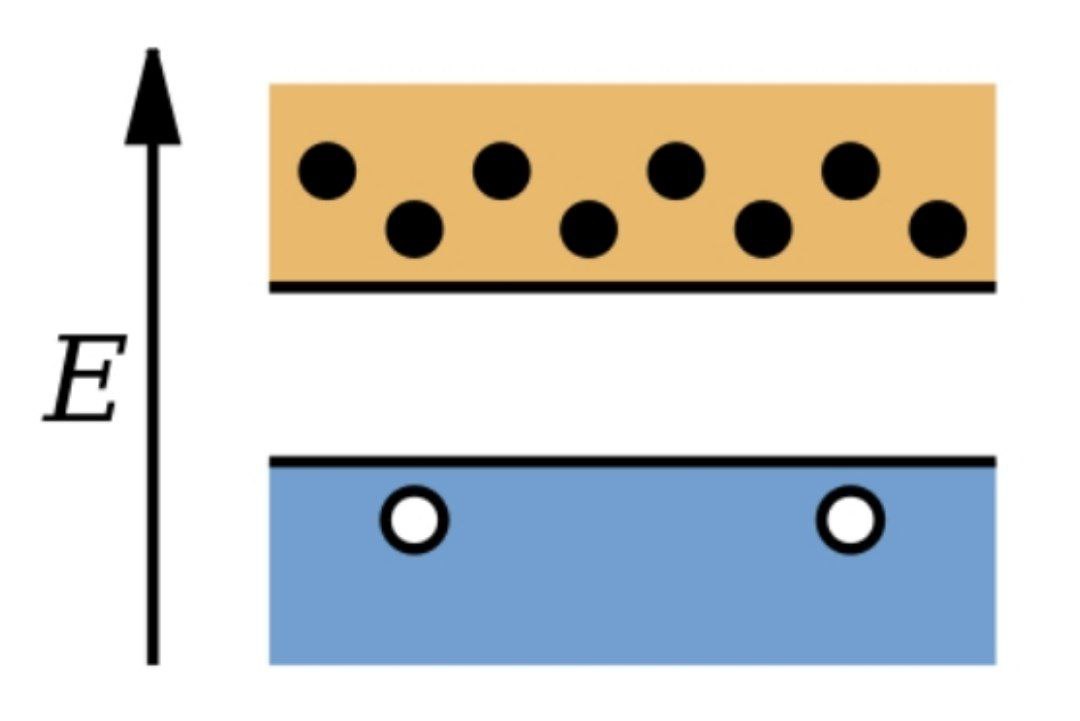
▶️ The image down below shows the band structure of a p-type semiconductor. Dark circles in the conduction band are electrons and light circles in the valence band are holes. The image shows that the holes are the majority charge carrier.
━━━━━━━━━━━━
☢ @Physics ⚡| @Education 📖
▶️ Examples: phosphorus, arsenic, antimony, etc.
▶️ The image down below shows the band structure of a p-type semiconductor. Dark circles in the conduction band are electrons and light circles in the valence band are holes. The image shows that the holes are the majority charge carrier.
━━━━━━━━━━━━
☢ @Physics ⚡| @Education 📖
👍31❤17🔥8