Apple has announced the biggest change heading to its Mac computers in 14 years: the dumping of Intel Inside.
The company is ditching Intel’s traditional so-called x86 desktop chips for Apple’s own processors based on ARM designs - those used in smartphones and mobile tablets, including the iPhone and iPad.
The Guardian
The company is ditching Intel’s traditional so-called x86 desktop chips for Apple’s own processors based on ARM designs - those used in smartphones and mobile tablets, including the iPhone and iPad.
The Guardian
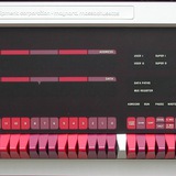
PDP-11🚀
The chapter from the upcoming Vivienne Sze book " Efficient Processing of Deep Neural Networks" http://eyeriss.mit.edu/2020_efficient_dnn_excerpt.pdf * Processing Near Memory * Processing in memory * Processing in the Optical Domain * Processing in Sensor
efficient_proceeding_of_dnn.pdf
20.4 MB
The fantastic book is finally generally available now!
Efficient Processing of Deep Neural Networks
This tutorial covers all aspects of model software and hardware design related to the this topic. Explain very key concepts of weight/output/input/row stationarities and dataflow, power budget tradeoffs and hardware-software co-design aspects.
Efficient Processing of Deep Neural Networks
This tutorial covers all aspects of model software and hardware design related to the this topic. Explain very key concepts of weight/output/input/row stationarities and dataflow, power budget tradeoffs and hardware-software co-design aspects.
Sorry guys, this channel is transforming into link-collection feed, but I promise to be back on track soon with brief summaries :)
https://www.electronicdesign.com/industrial-automation/article/21136402/smartnic-architectures-a-shift-to-accelerators-and-why-fpgas-are-poised-to-dominate
https://www.electronicdesign.com/industrial-automation/article/21136402/smartnic-architectures-a-shift-to-accelerators-and-why-fpgas-are-poised-to-dominate
Bluspec Haskell is an open-source framework, yet another High Level Hardware Description Language, but now based on Haskell
Jonathan Ross, hardware AI startup Groq founder and ex-Google TPU developer, claims that it was used on initial stages of TPU design. It looks like Groq is also actively using it
https://www.linkedin.com/in/jonathan-ross-12a95156/
Bluespec research note
https://arxiv.org/pdf/1905.03746.pdf
The latest version of bluespec Compiler can be found here
https://github.com/B-Lang-org/bsc
And here's the tutorial
https://github.com/rsnikhil/Bluespec_BSV_Tutorial/tree/master/Reference
Syntiant, a startup developing AI edge hardware for voice and sensor solutions, today closed a $35 million round. CEO Kurt Busch says the funds will be used to ramp up production throughout the remainder of 2020.
The one million parts shipped to date includes both NDP100 and NDP101 parts since the company’s first production orders in September 2019. Both are manufactured at UMC in Singapore
Syntiant’s NPD100 and NPD101 processors measure about 1.4 millimeters by 1.8 millimeters and can run models with over half a million parameters. Packing a general-purpose ARM Cortex-M0 processor paired with 128KB of RAM, the chips consume less than 140 microwatts and enable onboard firmware security and authentication, keyword training, and up to 64 output classifications.
The NPD100 and NPD101 — which initially targeted performance of around 20 TOPS (trillion floating-point operations) per watt — use hundreds of thousands of flash memory NOR cells that read and write data one word or byte at a time. The processor-in-memory architecture was proposed by CTO Jeremy Holleman, a researcher at the University of North Carolina in Charlotte, as far back as the 2014 International Solid-State Circuits Conference. Syntiant asserts that the architecture is ideal for executing massively parallel operations in deep learning at low power.
According to a report published by Meticulous Research, the speech and voice recognition hardware market is expected to reach $26.8 billion by 2025
Article on the EET
Syntiant Webpage
VentureBeat
Syntiant raises $35 million for AI speech-processing edge chips
Syntiant, a startup developing AI and machine learning edge hardware for voice processing, has raised $35 million in venture capital.
#nonhw
https://api.deepai.org/publication-download-pdf/can-your-ai-differentiate-cats-from-covid-19-sample-efficient-uncertainty-estimation-for-deep-learning-safety
SoA Deep Neural Networks and Bayesian Neural Networks failed to distinguish cat and chest X-Ray image.
https://api.deepai.org/publication-download-pdf/can-your-ai-differentiate-cats-from-covid-19-sample-efficient-uncertainty-estimation-for-deep-learning-safety
SoA Deep Neural Networks and Bayesian Neural Networks failed to distinguish cat and chest X-Ray image.
PDP-11🚀
Amazing lecture by Dave Patterson Three Generations of Tensor Processing Units (TPUs) https://www.youtube.com/watch?v=VCScWh966u4 See the comment section for the detailed table of content, very short TL;DR - TPU v1️⃣ (2015) project was done from the block…
DavePattersonTPUv3.pdf
1.8 MB
A DomainSpecific Supercomputer for Training Deep Neural Networks
Google supercomputer, 4096 TPU v3 chips in a 2D torus topology, wins MLPerf benchmark contest, the result table was published published on 29th of July.
Note also that it's probably the first TPU v4 public release. It currently shows with a pretty moderate result - 3.5 times slower than a winner.
But it has 8 times less chips (256) , so it looks like Google will beat it's own record very soon, whenever they upscale TPUv4 supercomputer up to 1024 chips.
Google Cloud Blog
Google wins MLPerf benchmark contest with fastest ML training supercomputer | Google Cloud Blog
Google set performance records in six out of the eight MLPerf benchmarks at the latest MLPerf benchmark contest
❓ Can I run my Neural Network on the FPGA?
❓ Does Vivado HLS run my CPP code on the FPGA?
❓ What is difference between OneAPI and Intel OpenCL?
❓ Vitis - is it a sort of HLS for VIvado, isn't it?
🤔
There are two main FPGA vendors today - Xilinx and Intel. Both of them released dozens of different software developer oriented tools during the last couple of year. All of them promises the same - run you software on FPGA in a few clicks.
😕 It's a bit tricky to get through all these marketing papers and understand the role of each new thing.
📖 Here's the paper which should navigate you through all these applications and IDEs.
📝 Feel free to comment it right in the Google docs
Google Docs
intel_xilinx_software
Xilinx and Intel FPGA software portfolio overview By Konstantin V. Join us t.me/pdp11ml Two main FPGA vendors, Xilinx and Intel (ex. Altera) offer a rich and quite wide portfolio of different tools with very similar names and description. This work covers…
The latest paper by David Patterson & Google TPU team reveals details of the world most efficient and one of the most powerful supercomputers for DNN Acceleration - TPU v3. The one which was used to train BERT.
We recommend that you definitely read the full text, but here are insights and tldr highlights
Key Insight:
The co-design of an ML-specific programming system (TensorFlow), compiler (XLA), architecture (TPU), floating-point arithmetic (Brain float16), interconnect (ICI), and chip (TPUv2/v3) let production ML applications scale at 96%–99% of perfect linear speedup and 10x gains in performance/ Watt over the most efficient general-purpose supercomputers.
More highlights:
🐣🐤🐔 Three generations
There are 3 generations of TPU now released, TPU v1 used fixpoint arithmetic and was used for inference only. TPU v2 and v3 operate in floating-point and used for training. TPU v4 results were presented in MLPerf summer release, but there is no public information available. The TPU architecture differs from CPU with
▪️ Two Dimensional array processing units (instead of 1D vector SIMDs in CPU)
▪️Narrower data (8-16 bits)
▪️ Drop complex CPU features - caches and branch prediction
🐮🤜🐤 Fewer cores per chip (two oxen vs 1024 chickens)
NVidia put thousands of CUDA cores inside their chip. TPU v3 has only 2 TensorCores per chip. It's way easier to generate a program for 2 beefier cores than to swarm of wimpier cores.
Each TensorCore includes the following units:-
▪️
▪️
▪️
▪️
▪️
🐱🐶❓ From inference to training chip
Key challenges on the way from inference chip V1 to training hardware V2
▪️ Harder parallelization
▪️ More computation
▪️ More memory
▪️ More programmability
▪️ Wider dynamic range of data
✂️🧮✂️ Brain Float
The compromised
🍩🧬⚡️ Torus topology and ICI
TPU v1 was an accelerator card for CPU 'based computer. TPUv2 and v3 are building blocks of the supercomputer. Chips connected with ICI interface, each running at ~500Gbits/s. ICU enables direct connection between chips, so no need of any extra interfaces. GPU/CPU based supercomputers have to apply NVLink and PCI-E inside computer chase and InfiniBand network and switches to connect them.
Chips in TPUv2 and v3 clusters are connected in 2D Torus topology (doughnut ) and achieve an unbelievable linear scale of performance growth with increasing of chips number.
🛠⚙️🖥 XLA compiler (to orchestrate them all)
TF programs are graphs of operations, where tensor-arrays are first-class citizens. XLA compiler front-end transforms the TF graph into an intermediate representation, which is then efficiently mapped into selected TPU (or CPU/GPU) architectures. XLA maps TF graph parallelism across hundreds of chips, TensorCores per chip, multiple units per core. XLA provides precise reasoning about memory use at every point in the program.
Young XLA compiler has more opportunities to improve than a more mature CUDA stack.
🌲🐰🦊 Green Power (Forest animals approves)
TPU v3 supercomputer already climbed on the 4th row of TOP500 ranking, but what is remarkable - it demonstrates an overwhelming 146.3 GFLops/Watt performance. The nearest competitor has 10 times and lower number.
Original Paper
A Domain Specific Computer for training DNN
We recommend that you definitely read the full text, but here are insights and tldr highlights
Key Insight:
The co-design of an ML-specific programming system (TensorFlow), compiler (XLA), architecture (TPU), floating-point arithmetic (Brain float16), interconnect (ICI), and chip (TPUv2/v3) let production ML applications scale at 96%–99% of perfect linear speedup and 10x gains in performance/ Watt over the most efficient general-purpose supercomputers.
More highlights:
🐣🐤🐔 Three generations
There are 3 generations of TPU now released, TPU v1 used fixpoint arithmetic and was used for inference only. TPU v2 and v3 operate in floating-point and used for training. TPU v4 results were presented in MLPerf summer release, but there is no public information available. The TPU architecture differs from CPU with
▪️ Two Dimensional array processing units (instead of 1D vector SIMDs in CPU)
▪️Narrower data (8-16 bits)
▪️ Drop complex CPU features - caches and branch prediction
🐮🤜🐤 Fewer cores per chip (two oxen vs 1024 chickens)
NVidia put thousands of CUDA cores inside their chip. TPU v3 has only 2 TensorCores per chip. It's way easier to generate a program for 2 beefier cores than to swarm of wimpier cores.
Each TensorCore includes the following units:-
▪️
ICI(Inter Core Interconnects) - connect core across different chips- ▪️
HBM, stacked DRAM on the same interposes substrate- ▪️
Core Sequencer - manages instructions and performs scalar operations- ▪️
Vector Processing Unit, performs vectors operation for 1D and 2D vectors- ▪️
Matrix Multiply Unit (MXU) 🐱🐶❓ From inference to training chip
Key challenges on the way from inference chip V1 to training hardware V2
▪️ Harder parallelization
▪️ More computation
▪️ More memory
▪️ More programmability
▪️ Wider dynamic range of data
✂️🧮✂️ Brain Float
IEEE FP16 and FP32 use (1+8+23) and (1+5+7) bits for the sign, exponent, and mantissa values respectively. In practice, DNN doesn't need mantissa precision of FP32, but the dynamic range of FP16 is not enough. Using of FP16 also requires loss scaling.The compromised
bf16 keeps the same 8 bits for exponent, as FP32, but reduced mantissa - only 7 bits instead of 23. BF16 delivers reducing space usage and power consumption with no loss scaling in software required. 🍩🧬⚡️ Torus topology and ICI
TPU v1 was an accelerator card for CPU 'based computer. TPUv2 and v3 are building blocks of the supercomputer. Chips connected with ICI interface, each running at ~500Gbits/s. ICU enables direct connection between chips, so no need of any extra interfaces. GPU/CPU based supercomputers have to apply NVLink and PCI-E inside computer chase and InfiniBand network and switches to connect them.
Chips in TPUv2 and v3 clusters are connected in 2D Torus topology (doughnut ) and achieve an unbelievable linear scale of performance growth with increasing of chips number.
🛠⚙️🖥 XLA compiler (to orchestrate them all)
TF programs are graphs of operations, where tensor-arrays are first-class citizens. XLA compiler front-end transforms the TF graph into an intermediate representation, which is then efficiently mapped into selected TPU (or CPU/GPU) architectures. XLA maps TF graph parallelism across hundreds of chips, TensorCores per chip, multiple units per core. XLA provides precise reasoning about memory use at every point in the program.
Young XLA compiler has more opportunities to improve than a more mature CUDA stack.
🌲🐰🦊 Green Power (Forest animals approves)
TPU v3 supercomputer already climbed on the 4th row of TOP500 ranking, but what is remarkable - it demonstrates an overwhelming 146.3 GFLops/Watt performance. The nearest competitor has 10 times and lower number.
Original Paper
A Domain Specific Computer for training DNN
🤔🌳🏃♂️ Decision trees accelerating
One would be surprised, but DNNs do not exhaust the list of ML algorithms. In fact, few businesses can find an application of CV or NLP, few have a significant amount of speech or photo data, where DNN shows SOTA results.
But most of them have a huge amount of irregular table data - financial market prices, customer data, base station activity logs, or windmills breakdown statistics.
And that's where decision trees get up on stage. There are 3 major frameworks on the market nowadays, who provides frameworks for training ensembles of decision trees with gradient boosting. It's XGboost, CatBoost and LightGBM. Read here to learn more about them here or here
Due to the specific nature, good match between algorithm and hardware organizations, decision trees can be significantly accelerated on FPGA.
We will cover 2 stories here
🌝🇩🇪🥨 Xelera Decision Tree Acceleration
Germany-based startup Xelera offers FPGA devices as a hardware backend for decision trees inference acceleration. The company claims 700x both speedup and latency improvement. FPGA results were estimated on the cloud AWS F1 FPGA instances and on the Xilinx Alveo U50.
The secret as to why FPGAs perform so well on this class of workloads is their unique memory architecture, which consists of thousands of independent blocks of on-chip memory. This memory is not only highly parallel a key difference to the GPU memory is that it can handle highly parallel, irregular memory accesses very well.
🇺🇸🔬🎳 FPGAs for Particles classification
HLS4ML is an open-source framework from the Cornell University team, who is working in CERN, where FPGAs are used for trigger condition detection or particle classification.
HLS4ML generates an HLS description of the ML algorithm, which you may feed to the HLS synthesis tool (i.e. Vivado HLS) to generate an FPGA configuration file.
The recent paper describes how to use HLS4ML to generate FPGA firmware and host software for decision trees acceleration.
Taking as an example a multiclass classification problem from high energy physics, we show how a state-of-the-art algorithm could bedeployed on an FPGA with a typical inference time of 12 clock cycles (i.e., 60 ns at a clock frequency of 200 MHz)
🤓🤓🤖🤓🤓
How PCIe 5 and its Smart Friends Will Change Solution Acceleration
Nice article by Scott Schweitzer, Xilinx
Keynotes:
🥦PCI-E Gen5 offers not only throughput bandwidth doubling, but also Compute Express Link (CXL) and a Cache Coherent Interconnect for Accelerators (CCIX) promise to create efficient communication between CPUs and accelerators like SmartNIC or co-processors.
🕸 CCIX configurations include direct attached, switched topologies, and hybrid daisy chain. it can take memory from different devices, each with varying performance characteristics, pool it together, and map it into a single non-uniform memory access (NUMA) architecture. Then it establishes a Virtual Address space, enabling all of the devices in this pool access to the full range of NUMA memory
🥥 SmartSSDs, also known as computational storage, place a computing device, often an FPGA accelerator, alongside the storage controller within a solid-state drive. This enables the computing device in the SmartSSD to operate on data as it enters and exits the drive, potentially redefining both how data is accessed and stored.
👩🔬 SmartNICs, are a special class of accelerators that sit at the nexus between the PCIe bus and the external network. While SmartSSDs place computing close to data, SmartNICs place computing close to the network
👩👩👧👧 SmartNICs and DPUs (data processing units) that leverage PCIe 5 and CXL or CCIX will offer us richly interconnected accelerators that will enable the development of complex and highly performant solutions